|
Product Details:
|
| Name: | SFP C++ | Storage Temperature: | -40~85℃ |
|---|---|---|---|
| Operating Case Temperature: | 0~70℃ | Power Supply Voltage: | 3.1~3.5V |
| Application: | FTTB/FTTH/FTTO | Wavelength: | Tx 1310nm/Rx1490nm |
| High Light: | Tx 1310nm gpon sfp class c++,Rx1490nm gpon sfp class c++,Tx 1310nm gpon olt class c++ |
||
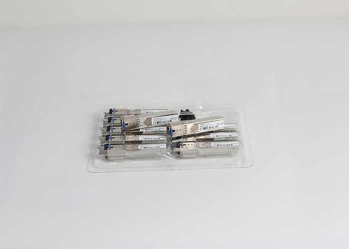
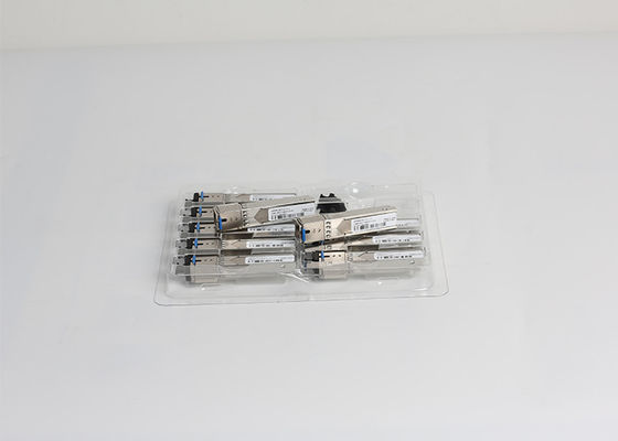
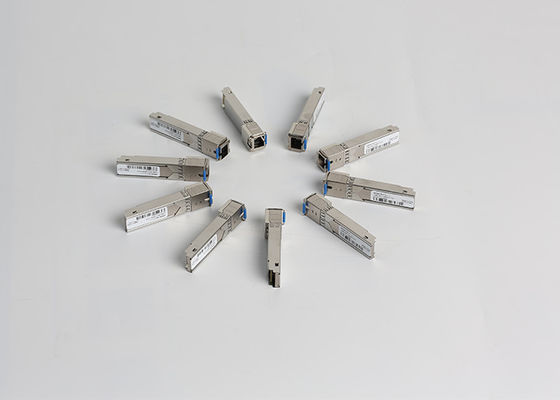
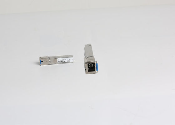
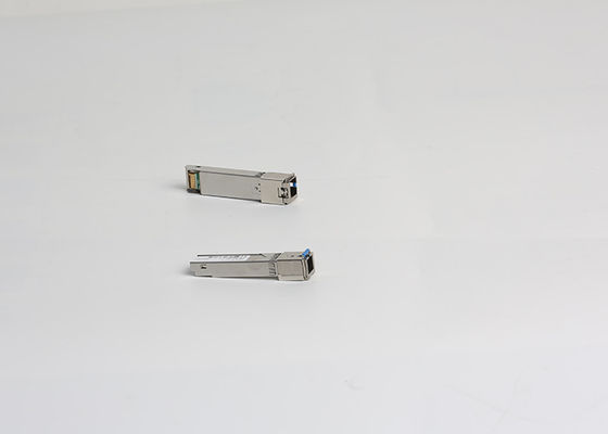
GPON Olt Sfp C++ Olt Transceiver 1490 Nm DFB Tx With Isolator
1. Features
2. Application
3. Function Diagram
![]()
4. Recommended Operating Conditions
| Parameter | Symbol | Min. | Max. | Unit | Notes |
| Storage Temperature | TSTG | -40 | 85 | °C | |
| Operating Case Temperature | TC | 0 | 70 | °C | ZP5432043-QCS |
| Operating Case Temperature | TC | 0 | 70 | °C | ZP5432043-QIS |
| Power Supply Voltage | VCC | 3.1 | 3.5 | V | |
| Total Power Supply Current | Icc | - | 500 | mA |
5. Transmitter Characteristics
| Parameter | Symbol | Min. | Typ. | Max. | Units | Notes |
| Optical Transmitter Power | P0 | 7 | - | 11 | dBm |
1 |
| Optical Transmitter Power off | POFF | - | - | -39 | dBm | |
| Output Center Wavelength | λ | 1480 | - | 1500 | nm | |
| Output Spectrum Width | Δλ | - | - | 1.0 | nm | |
| Side Mode Suppression Ratio | SMSR | 30 | - | - | dB | |
| Extinction Ratio | ER | 9 | - | - | dB | |
| Optical Rise Time | - | - | - | 160 | ps | |
| Optical Fall Time | - | - | - | 160 | ps | |
| Optical Eye Diagram | Compliant with ITU-T G.984.2 Mask | |||||
| Tolerence to Tx Back Reflection | - | -15 | - | - | dB | |
| Data Rate | - | - | 2.488 | - | Gb/s | |
| Differential Input Voltage | VPP | 300 | - | 1200 | mV | |
| Differential Input Impedance | ZIN | 80 | 100 | 120 | ohm | |
| Tx_fault Output Voltage- High | VIH | 2.4 | - | - | V | |
| Tx_fault Output Voltage- Low | VIL | - | - | 0.4 | V | |
| Tx_Dis Input Voltage- High | VIH | 2.0 | - | - | V | |
| Tx_Dis Input Voltage- Low | VIL | - | - | 0.8 | V | |
6. Receiver Characteristics
| Parameter | Symbol | Min. | Typ. | Max. | Units | Notes |
| Wavelength of Operation | - | 1260 | - | 1360 | nm | - |
| Data Rate | - | - | 1.244 | - | Gb/s | - |
| Sensitivity | Sen | - | - | -32 | dBm | 1 |
| Saturation Optical Power | Sat | -8 | - | - | dBm | 1 |
| Burst Packet Detect sensitivity | - | - | - | -32 | dBm | 1 |
| Receiver Reflectance | - | - | - | -12 | dB | |
| Receiver Burst-mode Dynamic Range | - | 15 | - | - | dB | 2 |
| Data Output Differential Swing | - | 400 | - | 1600 | mV | |
| RSSI accuracy | - | -3 | - | 3 | dB | 3 |
| BPD Output Voltage- High | VIH | 2.4 | - | - | V | 4 |
| BPD Output Voltage- Low | VIL | - | - | 0.4 | V | 4 |
| Guard Time | TGUARD | - | 32 | - | bits | - |
| Rest Width | TRESET | 16 | - | bits | ||
| Reset-Low | 0 | 0.8 | V | |||
| Reset-High | 2.0 | Vcc | V | |||
| Receiver Amplitude Recovery Time | TRECOVERY | - | 24 | 32 | bits | |
| Signal Detect De-Asset Time | 12.8 | ns | ||||
| Signal Detect Assert Time | 50 | ns | ||||
| Optical Signal During Time | TONT EN_DUR | 300 | - | - | ns | 5 |
| RSSI Trigger Delay | TD | 0 | - | 3000 | Ns | 6 |
| RSSI Trigger Width | TW | 300 | - | TONT EN_DUR | ns |
Note 1: Measured with 1310nm, 1.244Gbps PRBS223-1 burst-mode optical input, ER=10dB, BER=1x10⁻¹⁰;
Single burst packet length is 40us and packet interval is 40us.
Note 2: Input optical power level difference of adjacent burst packets.
Note 3: Receiver optical power ranged from -8dBm to -28dBm, measured with 1310nm, 1.244Gbps PRBS27-1
burst-mode optical input, ER=10dB, 50%duty cycle.
Note 4: BPD assert low when module receive “Reset” signal, assert high when burst package is detected and latch
to high state until next “Reset” signal.
Note 5: For RSSI Measurement
Note 6: Refer to first bit of the preamble
7. Burst Mode Receiver Dynamic Range
![]()
8. Timing Parameter Definitions in Burst Mode Sequence
![]()
9. RSSI Timing Sequence
![]()
Contact Person: Miss. Doris Yao
Tel: 18872915494
Fax: 86-755-83151488